
PCB Design
What is PCB Design?
PCB design, or Printed Circuit Board design, is the process of creating a blueprint or layout for an electronic circuit on a flat board made of non-conductive material like fiberglass or epoxy resin. This circuit board contains various electrical components, such as resistors, capacitors, integrated circuits, and connectors, and it serves as a platform for connecting and interconnecting these components to enable electronic devices to function properly. PCB design involves specifying the placement of components, designing the pathways or traces that connect them, and ensuring that the design adheres to electrical, thermal, and mechanical requirements. The resulting design file is used in the manufacturing process to produce the physical circuit board, which is an essential part of countless electronic devices, from smartphones and computers to household appliances and automotive systems.
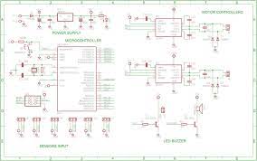
Schematic Design
Schematic Design is the initial stage of PCB design, where the blueprint of the electronic circuit is conceptualized and planned. During this phase, engineers and designers create a schematic diagram that illustrates the components, connections, and functionality of the circuit. It involves selecting the appropriate electronic components, such as resistors, capacitors, and integrated circuits, and representing them symbolically on the schematic. The connections between these components are defined, indicating how they interact electrically. Schematic Design is crucial for visualizing the circuit’s operation, ensuring that it meets the intended functionality, and laying the foundation for the subsequent stages of PCB design, including layout and prototyping.
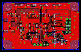
PCB Layout Design
PCB Layout Design is the second crucial stage in the PCB design process. During this phase, the electronic components and their connections, as outlined in the schematic design, are physically positioned on the circuit board. Designers carefully arrange the components while considering factors like signal integrity, thermal management, and board size constraints. They create the copper traces that connect these components, paying close attention to signal paths, power distribution, and ground planes to ensure optimal functionality and performance. The layout must also adhere to industry-specific standards and manufacturing requirements. Efficient PCB layout design is essential for minimizing signal interference, ensuring the reliability of the final product, and simplifying the manufacturing process.
Prototyping and Testing
The “Prototyping and Testing” stage in PCB design is a critical phase that comes after the schematic and layout design. During this stage, a physical prototype of the PCB is created based on the design files. This prototype allows designers and engineers to validate the functionality and performance of the circuit in real-world conditions. Rigorous testing is conducted to ensure that electrical connections are correct, components are properly placed, and the board operates according to specifications. Any issues or errors identified during testing are addressed, and necessary adjustments are made to the design. Prototyping and testing play a pivotal role in ensuring the reliability and quality of the final PCB, reducing the risk of costly errors in the manufacturing process and ultimately leading to the production of functional and dependable electronic devices.
Have any questions? Interested in our design services? Contact us to get started!


